- Language:
 English ▼
English ▼
ItemNo :
Lith-SD-01MOQ :
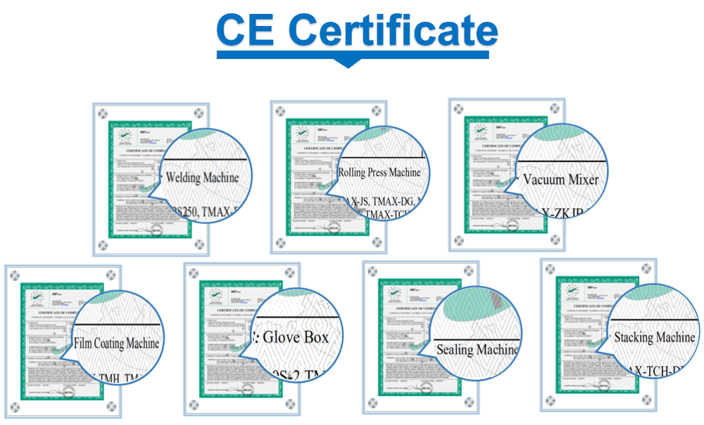
1Compliance:
CE CertifiedWarranty:
1 yearDelivery Time:
5 days
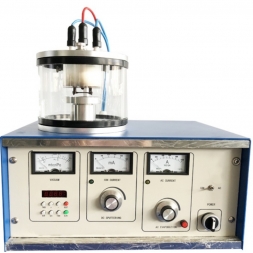
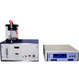
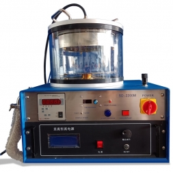
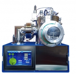
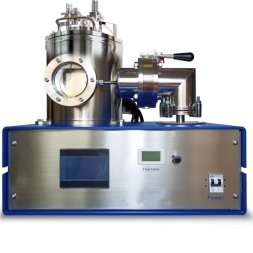
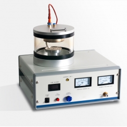
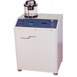
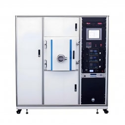
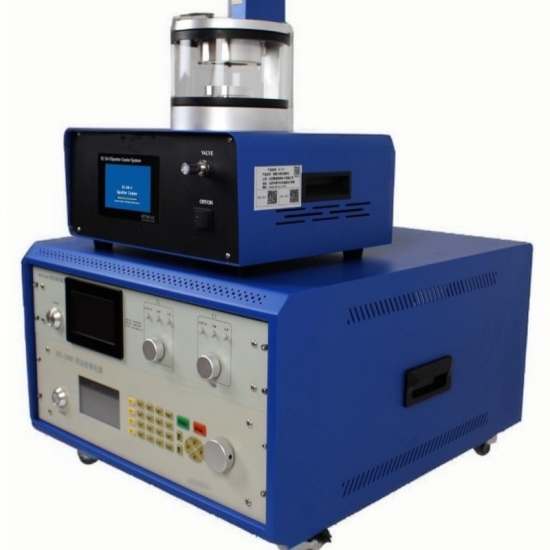
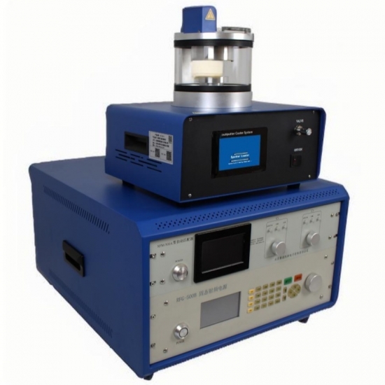
Model: Lith-SD-01-Metals & Non-Metals: Insulators, Semiconductors, Carbon-Based Thin Film Deposition
Product Specifications
|
Parameter |
Specification |
|
Model |
Lith-SD-01 |
|
Type |
RF Magnetron Sputtering System |
|
Chamber Size |
150 × 120 mm |
|
Target Material |
50 mm diameter (metals & non-metals, thickness: 1–2 mm) |
|
RF Power |
Adjustable (1–500 W) |
|
RF Frequency |
13.56 MHz |
|
Matching Network |
Automatic impedance matcher |
|
Sputtering Area |
50 mm |
|
Ultimate Vacuum |
5 Pa (base pressure) |
|
Process Gases |
Argon, nitrogen, and other inert gases (flow rate adjustable) |
|
Max. Deposition Rate |
8 nm/min |
· RF Power & Auto-Matching: 13.56 MHz RF with automatic impedance matching ensures stable sputtering of both conductive and insulating materials (e.g., oxides, ceramics).
· Broad Applications: Ideal for advanced thin-film research in semiconductors, optics, and functional coatings.
· Adjustable Inert Gas Flow: Supports Ar, N₂, and other inert gases for controlled deposition environments.
· High Purity Deposition: Base vacuum of 5 Pa minimizes contamination, ensuring high-quality film growth.
· Quick Target Change: Compatible with 50 mm targets (1–2 mm thick) for flexible material testing.
· Preset Process Recipes: Saves and recalls parameters for repeatable experiments and production.
· Max Deposition Rate: 8 nm/min with excellent film uniformity.
· Automated Matching: Reduces manual tuning and enhances process stability.
✔ Research & Development: Thin-film studies for semiconductors, dielectrics, and optical coatings.
✔ Small-Scale Production: Prototyping and specialized coating applications.
✔ Multi-Material Sputtering: Supports both metallic and non-metallic targets for diverse material systems.


![]()
![]()
![]()
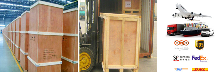
PACKAGE:
1 Standard exported package: Internal anticollision protection, external export wooden box packaging.
2 Shipping by express, by air, by sea according to customers' requirements to find the most suitable way.
3 Responsible for the damage during the shipping process, will change the damage part for you for free.
DELIVERY TIME: 15-20 days after confirming order,detail delivery date should be decided according to production season and order quantity

 Subscribe to us
 ONLINE
 +86 13174506016
 Louis@lithmachine.com
 +86 18559646958
 18659217588