- Language:
 English ▼
English ▼
ItemNo :
Lith-SD-JS02MOQ :
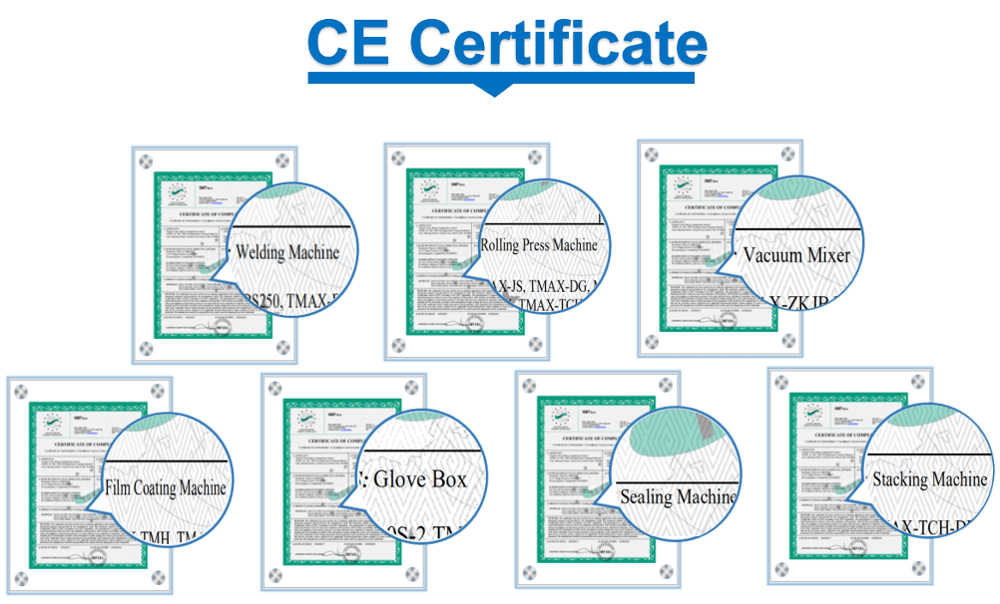
1Compliance:
CE CertifiedWarranty:
1 yearDelivery Time:
5 days
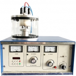
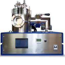
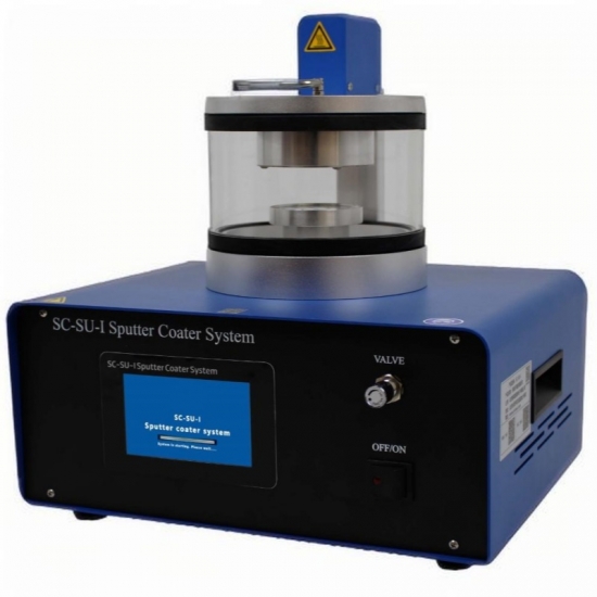
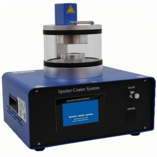
Model: Lith-SD-JS02-Sputtering System for Research Labs, Semiconductor Prototyping, and Optical Coating
Product Overview
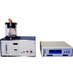
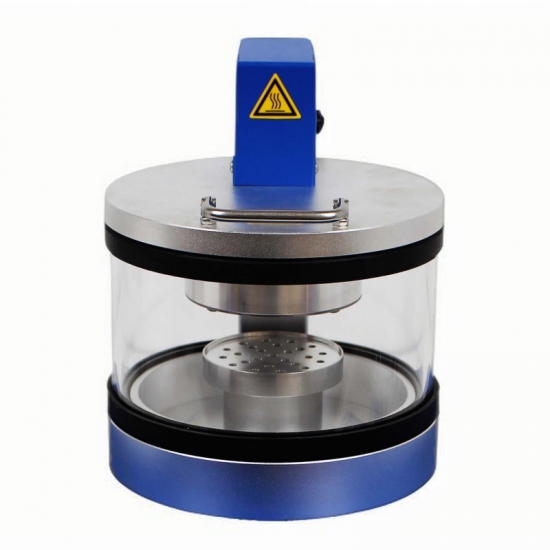
The Plasma Magnetron Sputtering System (Model: Lith-SD-JS02) is a compact, user-friendly instrument designed for high-quality thin film deposition. With a quartz chamber (150 × 120 mm) and a maximum sputtering rate of 8 nm/min, it is ideal for research and small-scale production requiring precise, uniform coatings. Compatible with inert gases (Ar, N₂) and versatile metal targets (Au, Ag, Pt, etc.), this system combines efficiency with advanced operational features.
|
Parameter |
Specification |
|
Quartz Chamber Size |
150 × 120 mm |
|
Sample Stage Size |
70 mm (diameter) |
|
Sputtering Area |
50 mm (diameter) |
|
Max. Vacuum Degree |
5 Pa |
|
Process Gases |
Argon, Nitrogen (flow rate adjustable) |
|
Max. Sputtering Rate |
8 nm/min |
|
Power Consumption |
200 W |
|
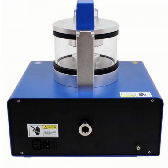
Dimensions (W×D×H) |
360 × 310 × 150 mm |
|
Operating Temperature |
0–40°C |
|
Relative Humidity |
< 85% |
|
Installation |
Horizontal desktop placement |
1. Intuitive Control & Monitoring
4.3" color touchscreen with graphical interface for real-time display of sputtering current, voltage, and vacuum levels.
2. Flexible Gas & Target Options
Adjustable inert gas flow (Ar/N₂) and support for 50 mm diameter metal targets (1–2 mm thickness), enabling quick material swaps and process reproducibility.
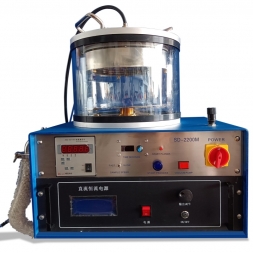
3. Modular & User-Centric Design
·Split-type quartz chamber for easy maintenance.
·Height-adjustable sample stage (±20 mm) with rotational alignment.
·Auto-venting post-sputtering simplifies sample handling.
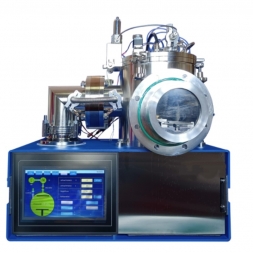
4. Compact & Reliable
·Space-saving footprint with multi-layered software protections for extended durability.
5. Uniform Film Quality
·Dense, homogeneous coatings compatible with noble and transition metals (Au, Ag, Pt, etc.).
· Research Labs: Thin film studies, surface engineering, and material science.
· Semiconductor Prototyping: Deposition of conductive/metallic layers.
· Optics & Electronics: Functional coatings for sensors or display components.
Note: Optimized for small substrates (≤50 mm) and low-to-medium throughput requirements.


![]()
![]()
![]()
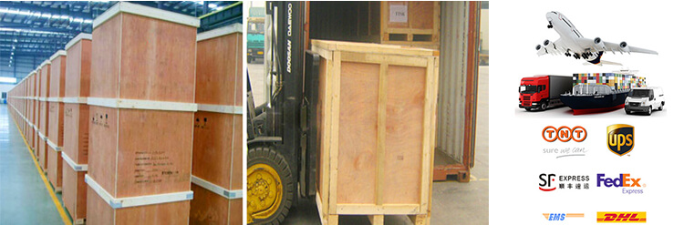
PACKAGE:
1 Standard exported package: Internal anticollision protection, external export wooden box packaging.
2 Shipping by express, by air, by sea according to customers' requirements to find the most suitable way.
3 Responsible for the damage during the shipping process, will change the damage part for you for free.
DELIVERY TIME: 15-20 days after confirming order,detail delivery date should be decided according to production season and order quantity

 Subscribe to us
 ONLINE
 +86 13174506016
 Louis@lithmachine.com
 +86 18559646958
 18659217588