- Language:
 English ▼
English ▼
ItemNo :
Lith-PC-JS12MOQ :
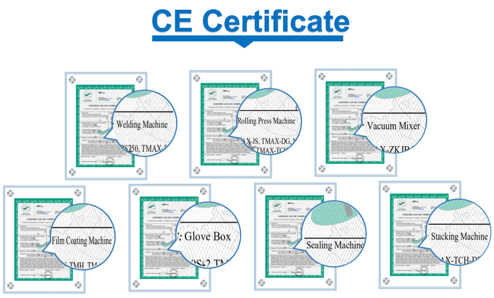
1Compliance:
CE CertifiedWarranty:
1 yearDelivery Time:
5 days
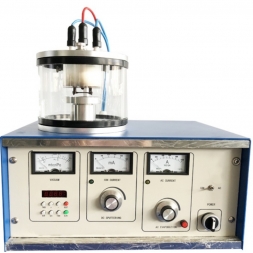
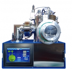
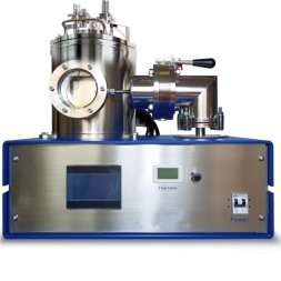
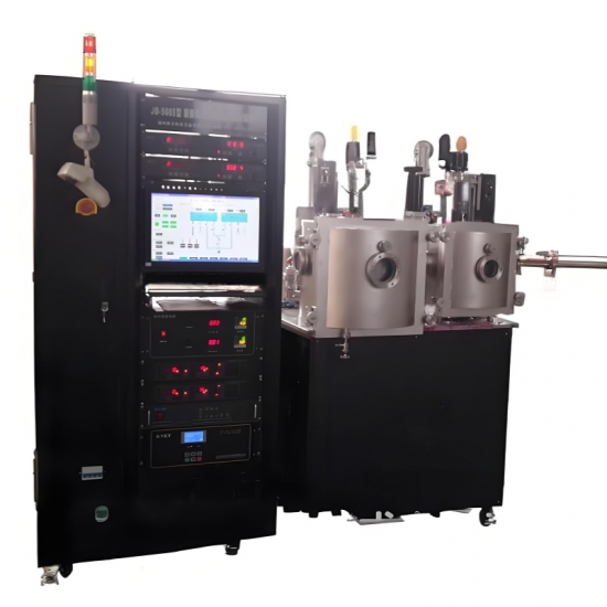
Model: Lith-PC-JS12-With Ion Source Cleaning & Assisted Sputtering
|
Category |
Description |
|
Application |
Preparation of nanoscale monolayer/multilayer functional films (hard coatings, metallic/semiconductor/dielectric films). Suitable for research labs, universities, and small-batch production. |
|
Key Features |
• Anode-layer ion source (cleaning + assisted deposition) • Reverse sputtering for adhesion enhancement • Automated PC-controlled process |
|
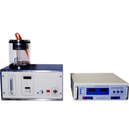
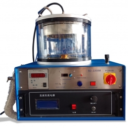
System Structure |
Sputtering chamber, 3 magnetron targets, heating stage, DC/RF power supplies, gas/pumping systems, vacuum measurement, control unit. |
|
Parameter |
Specification |
|
Chamber Design |
Vertical front-loading, stainless steel construction |
|
Base Vacuum |
≤5×10⁻⁵ Pa (sputtering chamber) |
|
Pumping Speed |
Recovers to 5×10⁻⁴ Pa in 100 min (via bypass valve + turbopump) |
|
Leak Rate |
≤5×10⁻⁷ Pa·L/s |
|
Pressure Rise Rate |
≤10 Pa after 12 hours (power off) |
|
Pumping System |
Domestic turbomolecular pump + mechanical pump |
|
Targets |
3 × 3-inch HV targets (2 standard, 1 strong magnetic field) |
|
Power Supplies |
• RF: 600 W, 13.56 MHz (auto-matching) • DC: 2 × 1000 W |
|
Target-to-Sample Distance |
40–120 mm (adjustable) |
|
Substrate Heating |
Max 450°C, programmable (rate/dwell time controllable) |
|
Film Thickness Uniformity |
±5% (e.g., Cu/Al: 4–5 μm; Ni/PTFE: 1–2 μm over 2-inch area) |
|
Adhesion Strength |
Survives 3 tape-peeling tests (glass/Si/ceramic) |
|
Pre-Cleaning |
Reverse sputtering + anode-layer ion source |
|
Gas Control |
2 MFCs (Ar + reactive gases), MKS-brand, mixing enabled |
|
Baking |
IR heating, max 150°C |
|
Safety |
Water/power failure interlocks, anti-misoperation protection |
|
Automation |
PC-controlled (target switching, substrate rotation, temperature) |
|
Feature |
Benefit |
Target Applications |
|
Ion Source + Sputtering |
Ensures clean surfaces and high adhesion |
Semiconductor films, optical coatings |
|
Multi-Mode Deposition |
Supports DC/RF, reactive sputtering, multilayers |
Research on novel functional materials |
|
Precise Automation |
Reduces human error, improves reproducibility |
Small-batch prototyping, academic labs |
|
Rapid Pumping |
Minimizes downtime between runs |
High-throughput R&D environments |
Key Features & Suitability
· High-Precision Deposition: Ensures uniform, high-adhesion films for research and prototyping.
· Multi-Functional Cleaning: Combines ion source + reverse sputtering for optimal surface preparation.
· Flexible Configuration: Supports DC/RF modes, multilayer films, and reactive sputtering.
· User-Friendly Automation: PC-controlled workflow reduces manual errors.
Ideal for: Advanced material research, semiconductor labs, and functional coating development requiring reproducible, high-quality thin films.

![]()
![]()
![]()
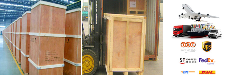
PACKAGE:
1 Standard exported package: Internal anticollision protection, external export wooden box packaging.
2 Shipping by express, by air, by sea according to customers' requirements to find the most suitable way.
3 Responsible for the damage during the shipping process, will change the damage part for you for free.
DELIVERY TIME: 15-20 days after confirming order,detail delivery date should be decided according to production season and order quantity

 Subscribe to us
 ONLINE
 +86 13174506016
 Louis@lithmachine.com
 +86 18559646958
 18659217588