- Language:
 English ▼
English ▼
ItemNo :
Lith-ZK-JS05MOQ :
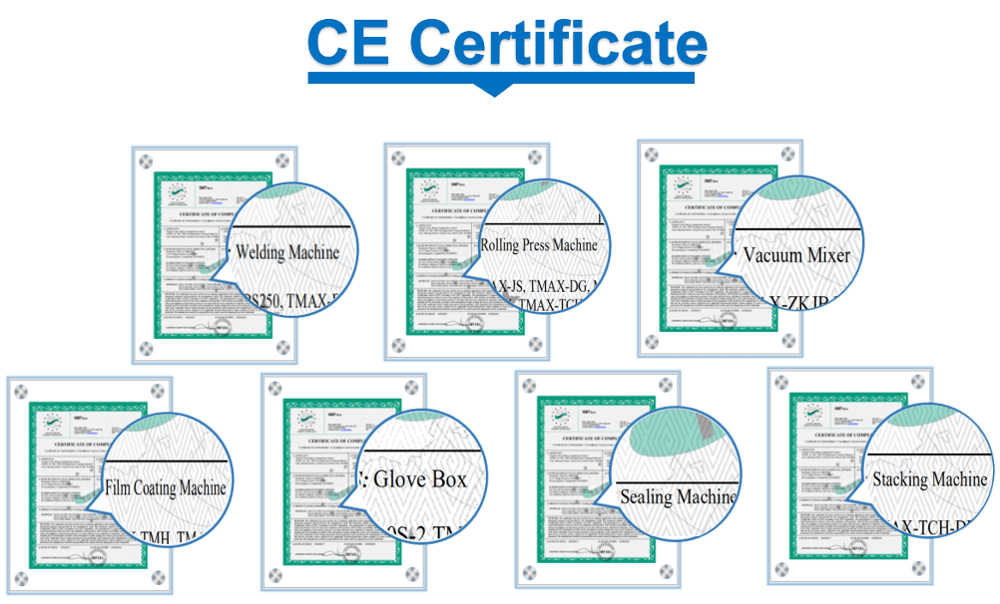
1Compliance:
CE CertifiedWarranty:
1 yearDelivery Time:
5 days
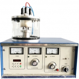
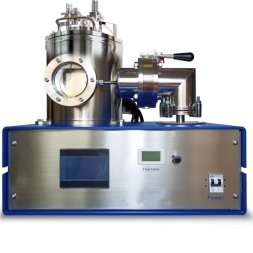
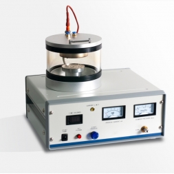
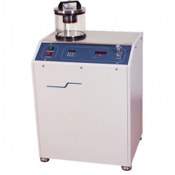
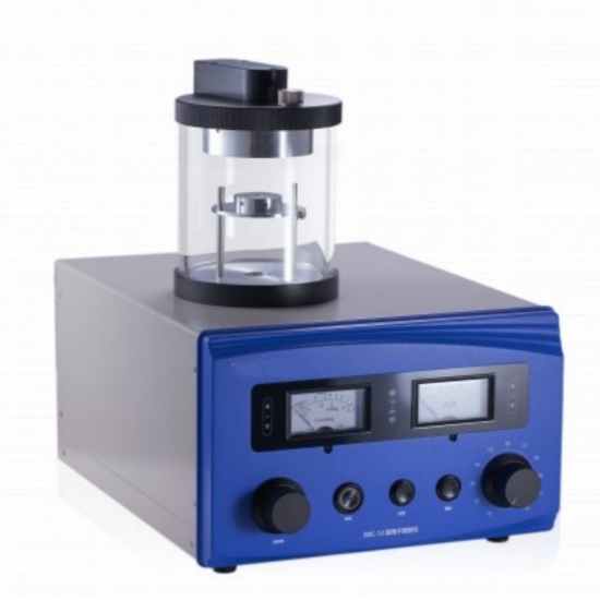
Model: Lith-ZK-JS05- Compact Ion Sputtering Coater
Overview
The Lith-ZK-JS05 Compact Ion Sputtering Coater is designed for depositing conductive gold films on samples for scanning electron microscopy (SEM). With user-friendly operation, it is an essential tool for sample preparation in small to medium-sized SEM laboratories.
· Gold ion sputtering for SEM sample coating.
· Compatible with target materials: Au, Pt, Cr, Ag, Ti, Cu, Ni, Au-Pd alloy, etc.
|
Category |
Specification |
|
Chamber Material |
Glass |
|
Chamber Dimensions |
Ø100 mm (diameter) × 130 mm (height) |
|
Sample Stage (Small) |
Ø40 mm (holds 6 sample cups simultaneously) |
|
Sample Stage (Large, Optional) |
Ø60 mm |
|
Gold Target Size |
Ø58 mm |
|
Vacuum Pump |
Two-stage direct-drive rotary vane pump (1 L/s) |
|
Vacuum Measurement |
Pirani gauge |
|
Vacuum Protection |
20 Pa with fine-adjustment gas inlet valve |
|
Working Gases |
Air / Argon (dedicated inlet with flow control) |
· Robust Design – Special sealing structure minimizes glass chamber damage.
· High Compatibility – Supports Au, Pt, Cr, Ag, Ti, Cu, Ni, and Au-Pd alloy targets.
· Precision Control – Adjustable gas flow and vacuum protection ensure uniform coatings.
· Efficient Workflow – Dual-stage platform allows batch processing (6 samples at once).
✔ SEM Sample Prep – Ideal for non-conductive specimen coating.
✔ Materials Research – Thin-film deposition for nanotechnology studies.
✔ Industrial QC – Reliable performance for repeatable conductive layering.

![]()
![]()
![]()
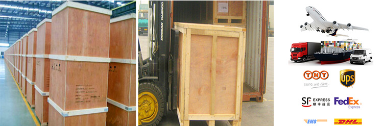
PACKAGE:
1 Standard exported package: Internal anticollision protection, external export wooden box packaging.
2 Shipping by express, by air, by sea according to customers' requirements to find the most suitable way.
3 Responsible for the damage during the shipping process, will change the damage part for you for free.
DELIVERY TIME: 15-20 days after confirming order,detail delivery date should be decided according to production season and order quantity

 Subscribe to us
 ONLINE
 +86 13174506016
 Louis@lithmachine.com
 +86 18559646958
 18659217588