- Language:
 English ▼
English ▼
ItemNo :
Lith-PD-JS04MOQ :
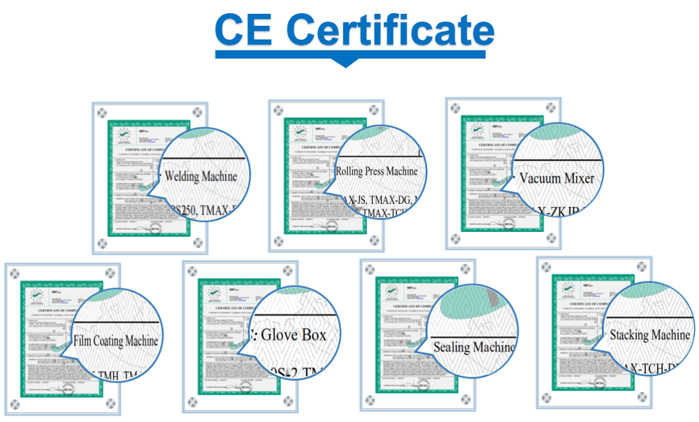
1Compliance:
CE CertifiedWarranty:
1 yearDelivery Time:
5 days
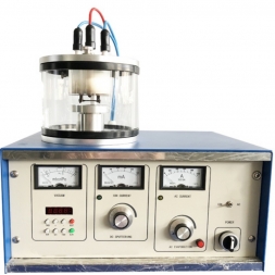
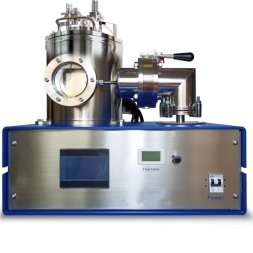
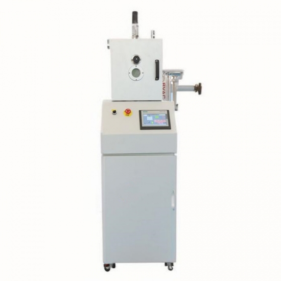
Model: Lith-PD-JS04-Adjustable Multi-Target System for Metal, Oxide, and Semiconductor
Product Overview
The Lith-PD-JS04 is a compact magnetron sputtering system designed for laboratory applications, including the deposition of metallic, oxide, dielectric, and semiconductor thin films, as well as the preparation of electrode materials for SEM sample coating. It is also suitable for educational purposes and pre-production process testing. With user-friendly operation, multifunctional capabilities, and high scalability, this system is ideal for academic research and industrial R&D.
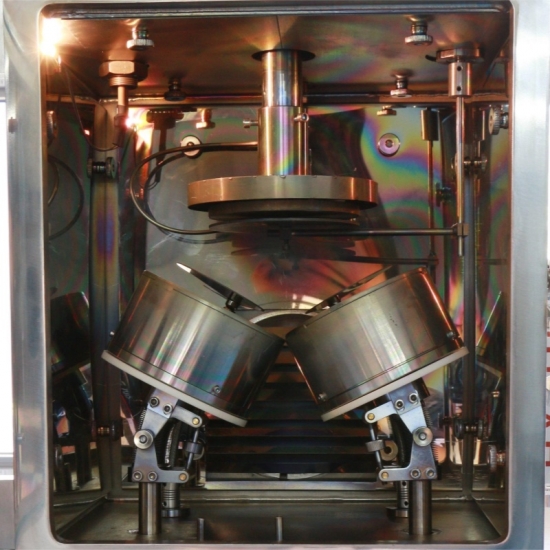
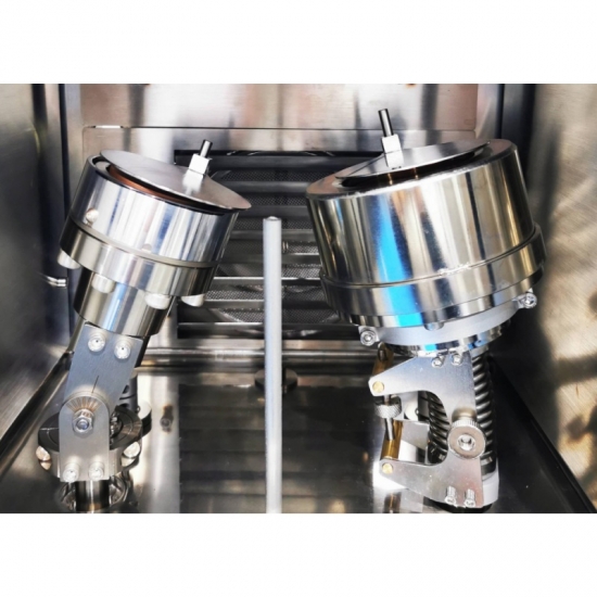
✔ Adjustable Co-Focal Sputtering Structure: The target gun height and angle are adjustable for optimized deposition.
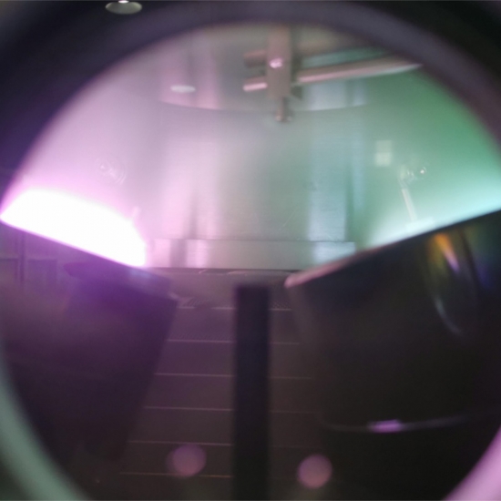
✔ Stable Gas Distribution: Process gases are introduced near the target surface, ensuring uniform reaction gas concentration throughout the vacuum chamber.
✔ Flexible Control Options: Supports both manual operation (Siemens PLC + touchscreen) and fully automatic control (computer + PLC).
✔ Precise Heating & Bias Control: The substrate stage supports heating up to 500°C (accuracy: ±3°C at 200°C, ±1.5°C at 500°C) and bias voltage up to -800V.
✔ High Uniformity: Film uniformity within ±3%~±5% over a 3-inch area.
|
Parameter |
Value |
|
Chamber Dimensions (L×W×H mm) |
300 × 300 × 380 |
|
System Dimensions (L×W×H mm) |
600 × 900 × 1900 |
|
Base Pressure |
≤5×10⁻⁵ Pa |
|
Pumping & Holding Capability |
≤8×10⁻⁴ Pa (30 min) / ≤8 Pa (12 hrs) |
|
Target Guns |
2 guns (2-inch or 3-inch optional) |
|
Sputtering Coverage |
2–4 inches |
✔ Advantages
· Co-focal sputtering design for precise film control.
· High uniformity (±3%~±5%) ensures consistent coating quality.
· Multi-functional for diverse thin-film research needs.
✔ Applications
· Academic Research: Thin-film studies, electrode fabrication, and SEM sample preparation.
· Advanced Materials: R&D in energy-related organic materials and novel processes.
This system excels in low-temperature, high-precision, and controllable thin-film deposition, making it a versatile tool for scientific and industrial innovation.


![]()
![]()
![]()
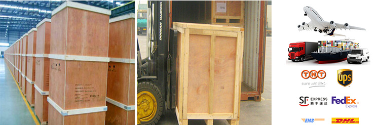
PACKAGE:
1 Standard exported package: Internal anticollision protection, external export wooden box packaging.
2 Shipping by express, by air, by sea according to customers' requirements to find the most suitable way.
3 Responsible for the damage during the shipping process, will change the damage part for you for free.
DELIVERY TIME: 15-20 days after confirming order,detail delivery date should be decided according to production season and order quantity

 Subscribe to us
 ONLINE
 +86 13174506016
 Louis@lithmachine.com
 +86 18559646958
 18659217588