Lith Corporation, founded in 1998 by a group of material science doctor from Tsinghua University, has now become the leading manufacturer of battery lab&production equipment. Lith Corporation have production factories in shenzhen and xiamen of China.This allows for the possibility of providing high quality and low-cost precision machines for lab&production equipment,including: roller press, film coater,mixer, high-temperature furnace, glove box,and complete set of equipment for research of rechargeable battery materials. Simple to operate, low cost and commitment to our customers is our priority.
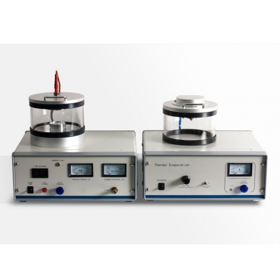
Evaporation and Sputtering Systems: Advanced Equipment for Precision Thin Film Deposition
Overview
Evaporation and sputtering systems are advanced physical vapor deposition (PVD) technologies designed for creating high-quality thin films on various substrates. These systems are widely used in research, development, and industrial applications where precision, uniformity, and reproducibility are essential. Evaporation involves heating a material until it vaporizes in a high-vacuum environment, allowing the vapor to condense on the substrate. Sputtering, on the other hand, utilizes ionized gas to bombard a target material, dislodging atoms that then deposit onto the substrate surface.
By combining evaporation and sputtering capabilities, these hybrid systems offer unparalleled flexibility, enabling deposition of metals, alloys, oxides, and certain compounds with precise control over film thickness, composition, and morphology. They are widely employed in electronics, optics, nanotechnology, and materials science laboratories, as well as small-scale production facilities.
Features
Modern evaporation and sputtering systems integrate a variety of features designed to optimize performance, efficiency, and ease of use:
1. High-Vacuum Chamber
A robust stainless-steel chamber capable of achieving ultra-high vacuum conditions (typically 10⁻⁵ to 10⁻⁷ torr) ensures minimal contamination and high film purity.
2. Dual Deposition Sources
These systems can be equipped with thermal evaporation sources and magnetron sputtering targets, allowing flexibility in material choice and deposition technique.
3. Substrate Motion and Rotation
Substrates are mounted on holders that can rotate, tilt, or oscillate during deposition, promoting uniform film thickness and surface coverage.
4. Thickness and Rate Monitoring
Quartz crystal microbalance (QCM) sensors and other monitoring devices provide real-time feedback on deposition rate and total film thickness, enabling precise control.
5. Digital Control and Automation
Programmable control panels allow operators to set deposition parameters such as power, substrate temperature, deposition rate, and process duration for repeatable results.
6. Safety and Maintenance Features
Vacuum interlocks, thermal protections, and modular construction facilitate safe operation and simplify maintenance.
Process
The operation of evaporation and sputtering systems involves several steps:
1. Substrate Preparation
Substrates must be cleaned thoroughly to remove dust, grease, or oxide layers that may reduce adhesion or affect film uniformity.
2. Chamber Evacuation
After loading the substrates and source materials, the chamber is sealed and evacuated to the desired vacuum level to minimize contamination and allow free travel of vaporized atoms.
3. Deposition
* Evaporation: The source material is heated using resistive, electron-beam, or other heating methods until it vaporizes and condenses onto the substrate.
* Sputtering: A plasma is generated by applying voltage to a target material in the presence of an inert gas (usually argon). Positive ions bombard the target, dislodging atoms that then deposit onto the substrate.
4. Monitoring and Control
Deposition rate, thickness, and uniformity are continuously monitored, and process parameters are adjusted as needed to achieve the desired film characteristics.
5. Completion and Venting
After reaching the target thickness, the system is cooled and vented, allowing safe removal of the coated substrates.
PVD Sputtering Coating
Applications
Evaporation and sputtering systems are used in diverse fields:
* Electronics and Semiconductor Industry: Deposition of conductive layers, electrodes, interconnects, and protective films.
* Optics: Fabrication of mirrors, anti-reflective coatings, optical filters, and multilayer coatings.
* Nanotechnology and Materials Research: Creation of thin films for experimental studies of electrical, magnetic, and optical properties.
* Renewable Energy: Coating of photovoltaic cells, transparent conductive films, and battery electrodes.
* Sample Preparation: Coating non-conductive substrates with conductive metals for scanning electron microscopy (SEM).
Advantages
Evaporation and sputtering systems provide several key advantages:
1. High Film Purity and Quality: Vacuum deposition ensures minimal contamination and excellent film adhesion.
2. Precise Thickness Control: Integrated monitoring systems allow accurate, repeatable control over film thickness.
3. Versatility: Capable of depositing a wide range of materials, including metals, alloys, oxides, and certain compounds.
4. Uniform Coating: Substrate rotation and optimized chamber design ensure consistent film coverage across complex geometries.
5. Flexibility in Process: Both evaporation and sputtering can be applied depending on material properties and desired film characteristics.
6. Laboratory and Industrial Adaptability: Systems are scalable from small benchtop research setups to larger production applications.
Conclusion
Evaporation and sputtering systems represent essential technology for precise, high-quality thin film deposition. By combining the complementary strengths of evaporation and sputtering techniques, these systems provide researchers and engineers with the ability to fabricate films with controlled thickness, uniformity, and composition.
From electronics and optics to nanotechnology and renewable energy, evaporation and sputtering systems enable advancements in material performance and device functionality. Their flexibility, reliability, and precision make them indispensable tools for both laboratory-scale research and small-scale production, supporting innovation across multiple scientific and industrial domains.
 English ▼
 Subscribe to us
 ONLINE
 +86 13174506016
 Louis@lithmachine.com
 +86 18559646958
 18659217588


